Precision MicroFab specializes in shaping vertical test probes, generally used for running electrical tests on integrated circuits.
Automated Micromachining of High-Precision Vertical Test Probes
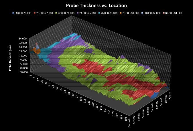
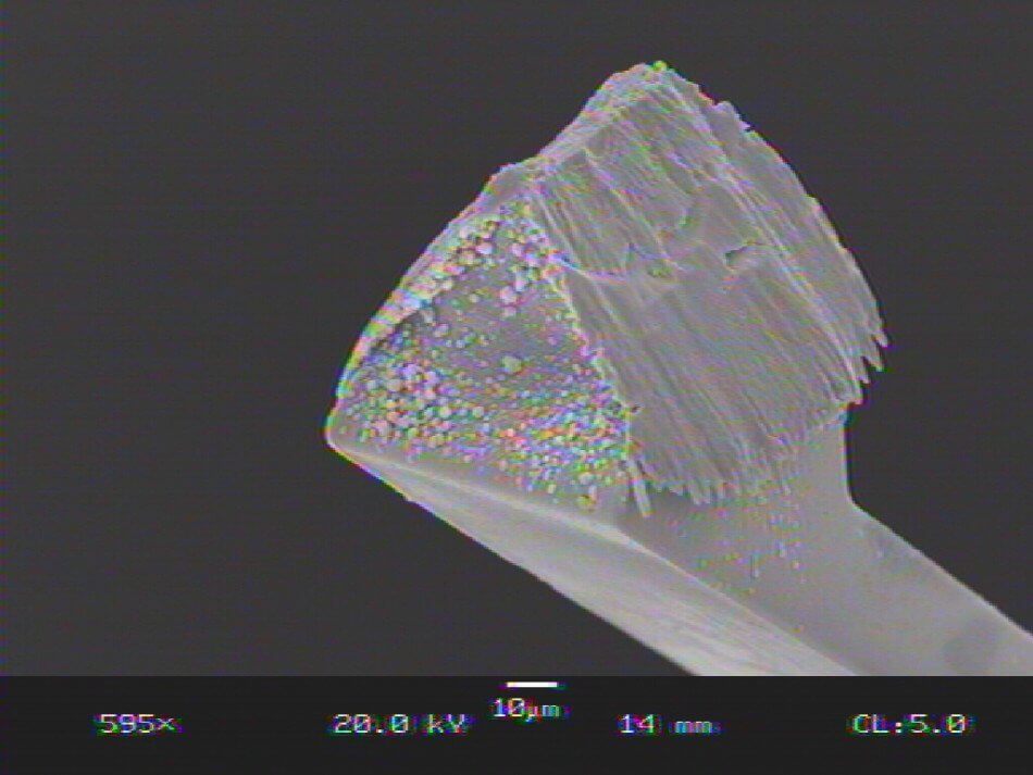
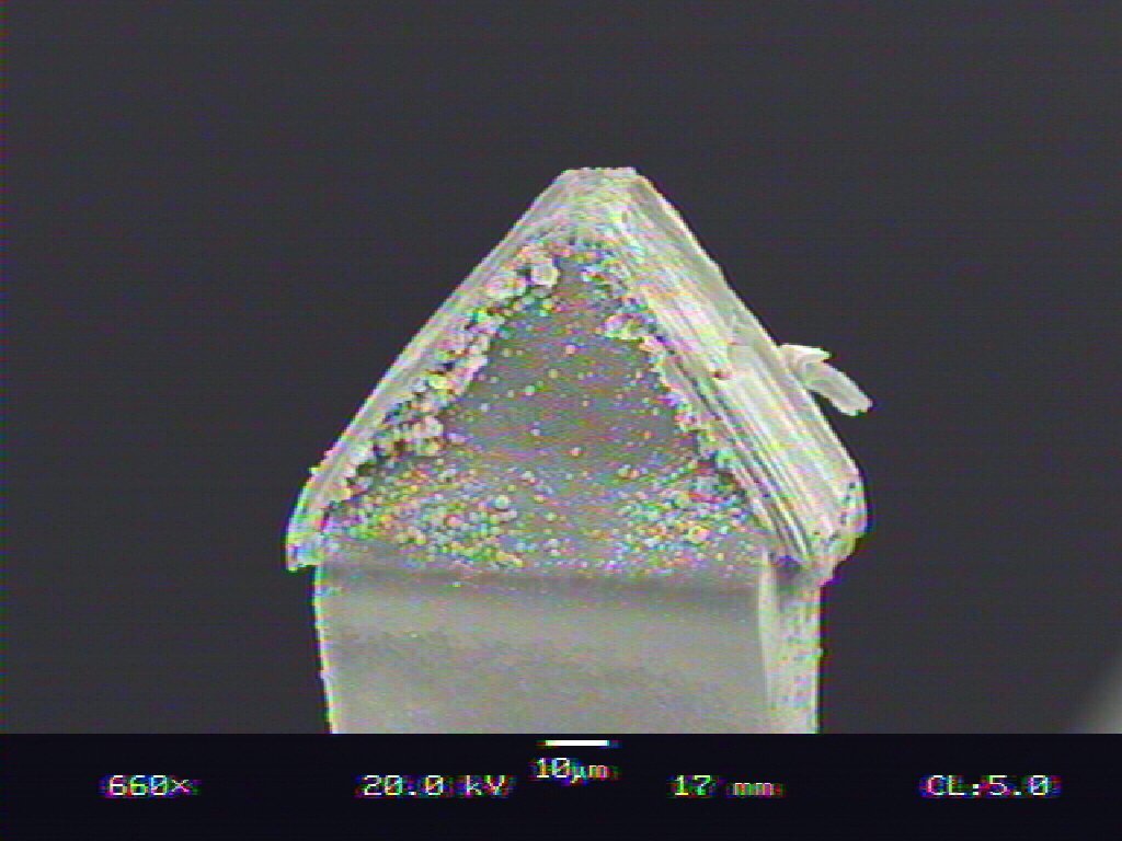
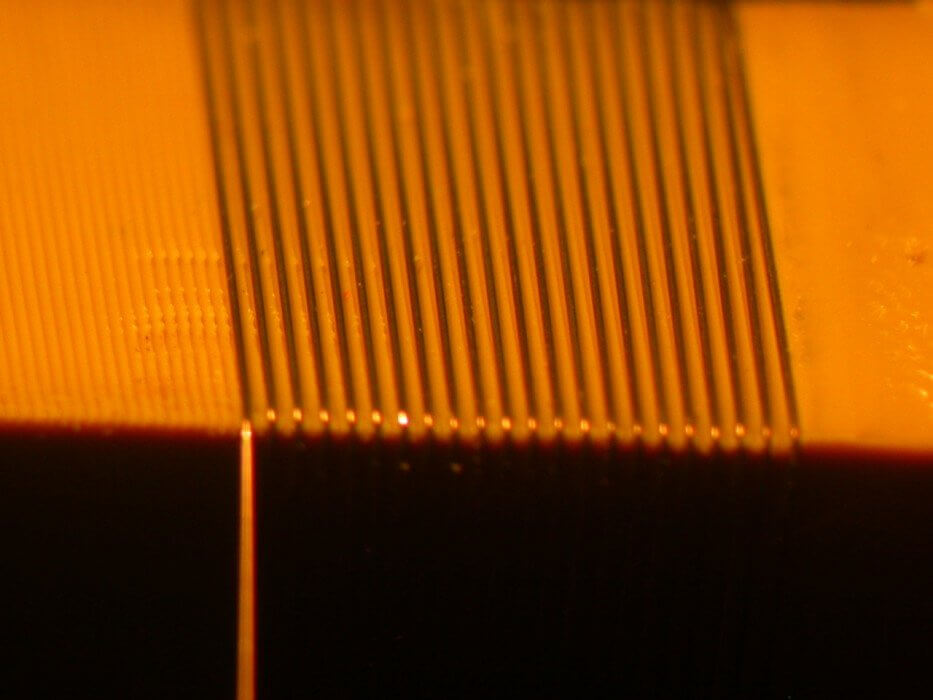
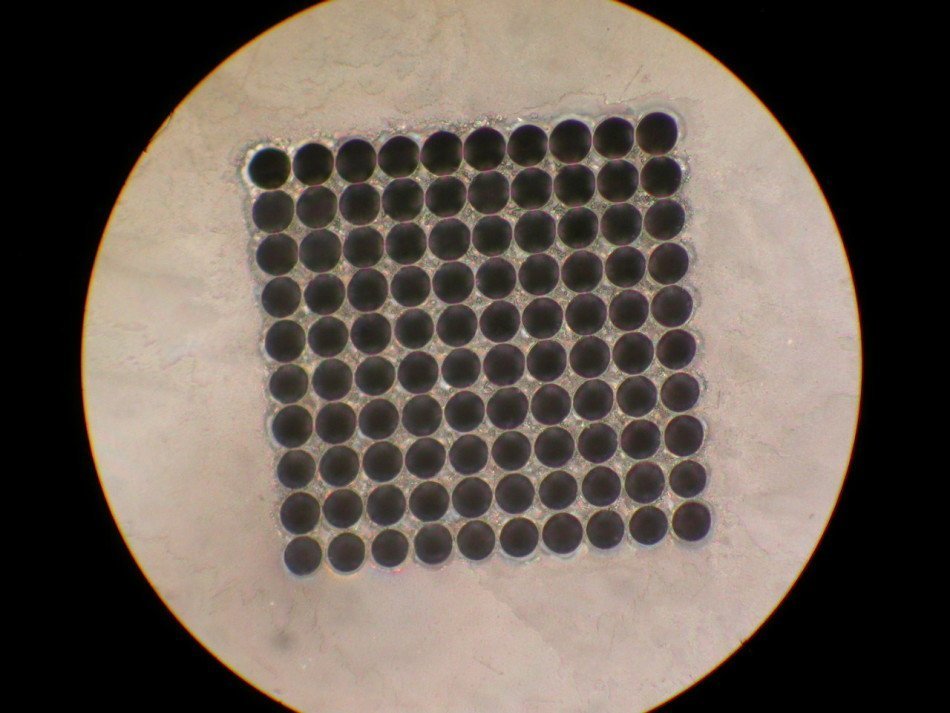
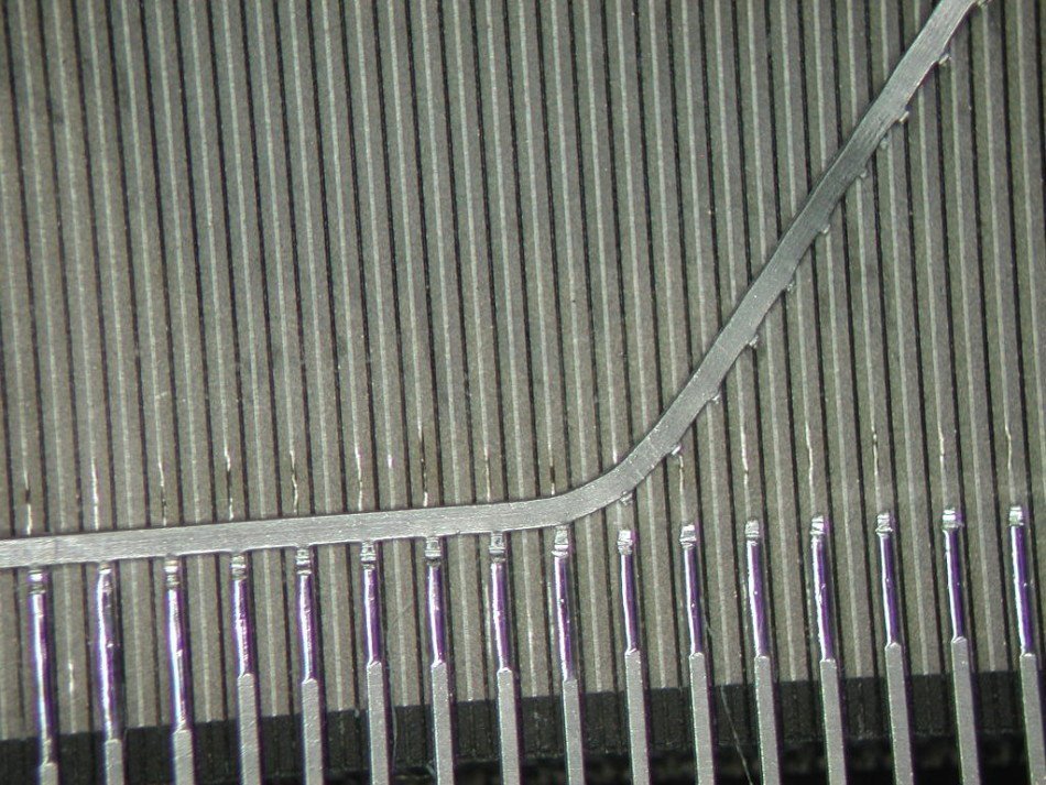
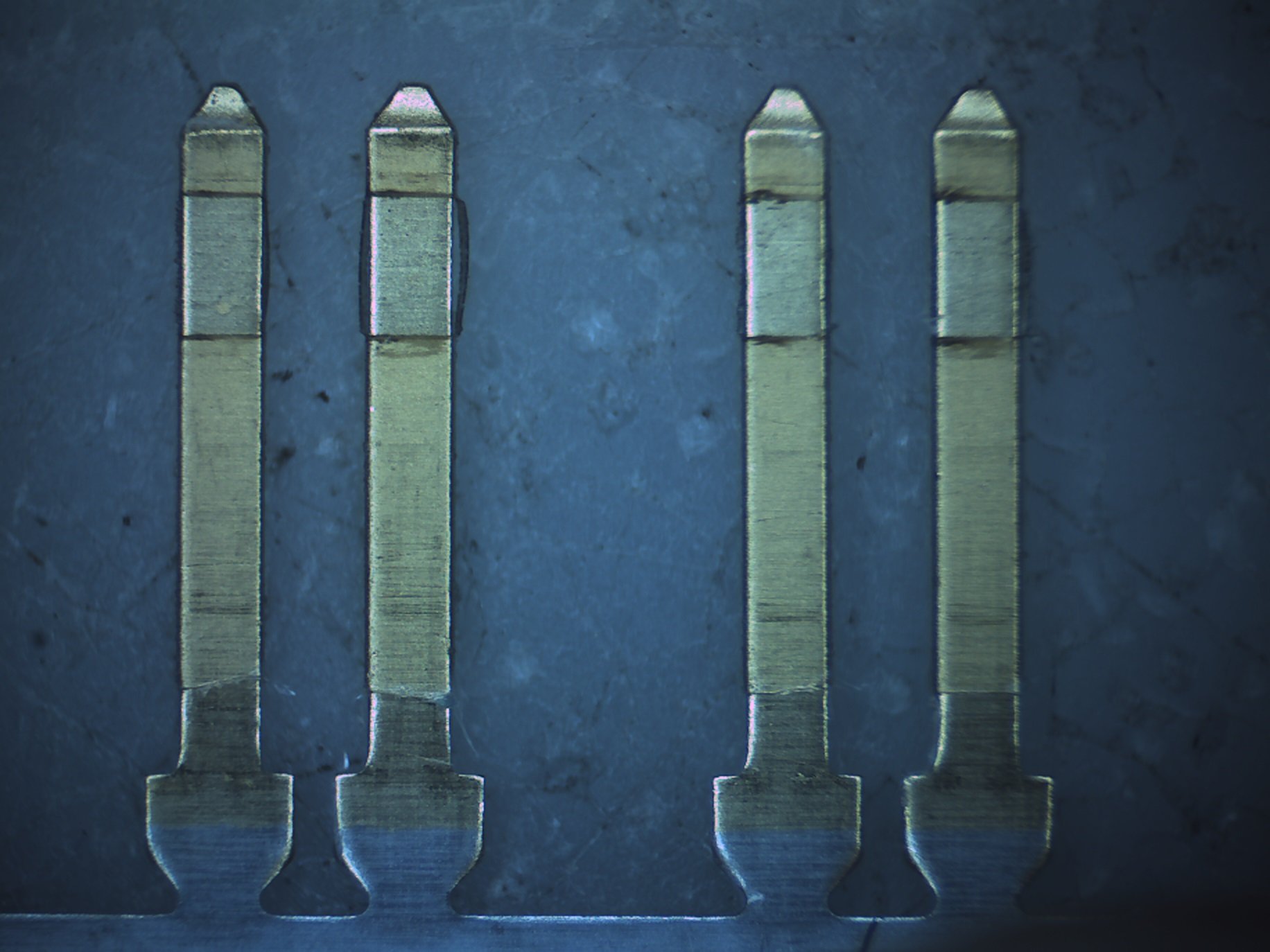
On this project, the probe tip had to scrub an oxide layer off the test area to minimize the electrical contact resistance (Cres). The probes were between 65 and 85 μm thick, but needed to be tapered down to consistent 6 μm truncated pyramids with a tolerance of +/- 2 μm.
In order to make these inconsistent and variably shaped probes consistent in size, this project was implemented with a high degree of automation, machine vision metrology, and customized fixturing. The top image is a three dimensional graph showing probe tip thicknesses across 9000 probes prior to shaping, and the bottom two images show the finished probes under the scanning electronic microscope.