- Selective coating removal (e.g., parylene windows) achieves clean, localized exposure areas to micron- scale tolerance, enabling downstream bonding, sensing, and electrical contact without mechanical damage.
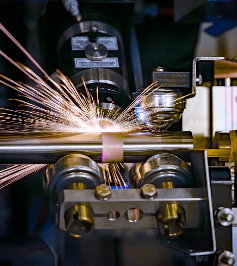
- Custom micro-positioning fixtures stabilize ultra-fine conductors for micro-soldering and assembly, improving yield, repeatability, and ergonomics at sub-millimeter scales.
- Artificial defect generation for CCIT enables validated leak-path controls and method development, accelerating device qualification and QA workflows.
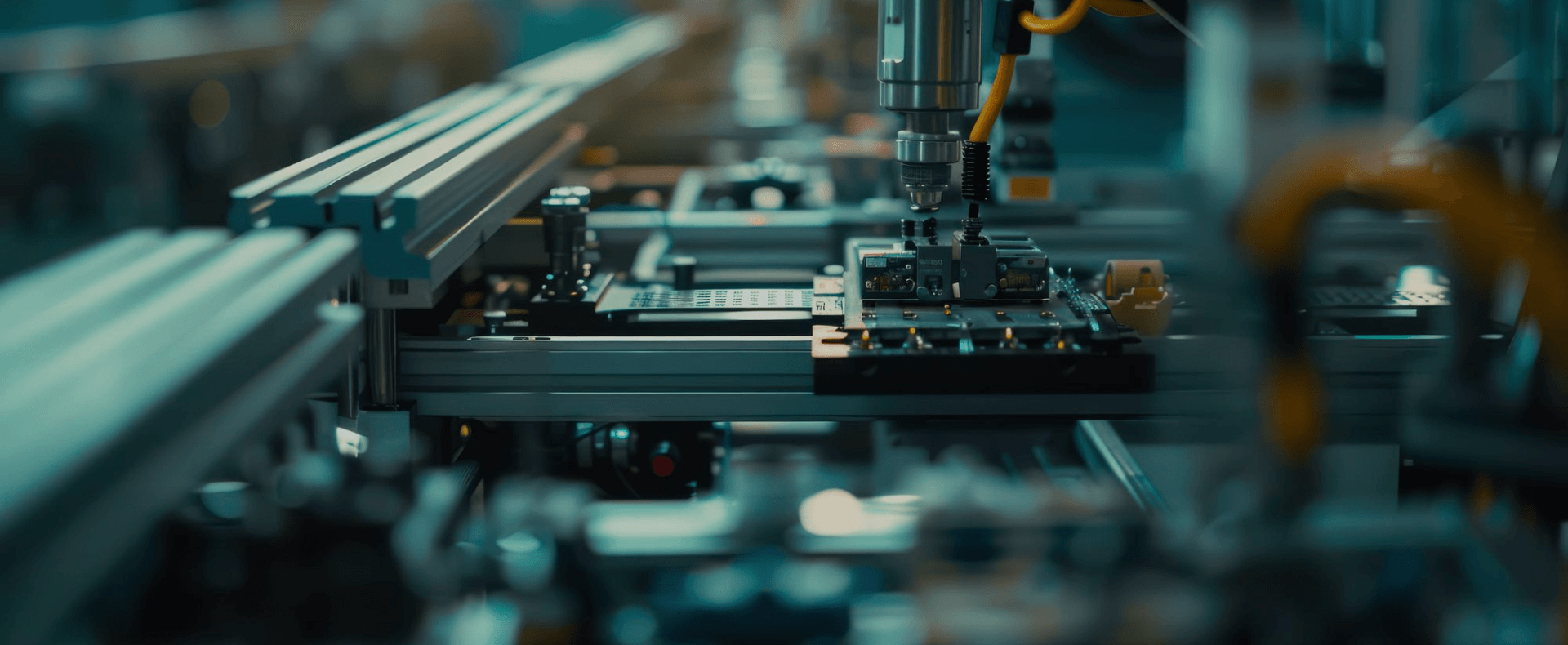
Miniaturization has increased complexity, tolerance demands, and the need for burr-free, stress-free features that conventional processes struggle to deliver at speed and cost. Laser-based microfabrication, micro 3D printing, and electroforming have expanded the process toolkit, but translating capability into validated production requires tight controls, metrology, and device-specific fixturing.
